Most Popular
-
1
1 in 3 Koreans live alone, family types becoming diverse

-
2
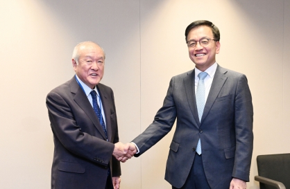
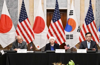
Korea, Japan finance chiefs vow to tame rampant FX market volatility
-
3
K-pop singer lost consciousness after being hit by foul ball, cancels show

-
4
K-pop group's manager dismissed for setting up spycam in theater dressing room
-
5
Contentious grain bill put directly to plenary meeting for vote


-
6
Korean Muslim YouTuber's plan to build mosque in Incheon goes viral
-
7
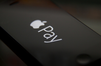
Why is Apple Pay struggling to get purchase in Korea?
-
8
Yoon's office denies considering liberal figures for key posts
-
9
Trilateral talks acknowledge ‘serious’ slumps of won, yen
-
10
[Today’s K-pop] BTS pop-up event to come to Seoul
![[Today’s K-pop] BTS pop-up event to come to Seoul](//res.heraldm.com/phpwas/restmb_idxmake.php?idx=644&simg=/content/image/2024/04/17/20240417050734_0.jpg&u=)


![[Today’s K-pop] BTS pop-up event to come to Seoul](http://res.heraldm.com/phpwas/restmb_idxmake.php?idx=644&simg=/content/image/2024/04/17/20240417050734_0.jpg&u=)
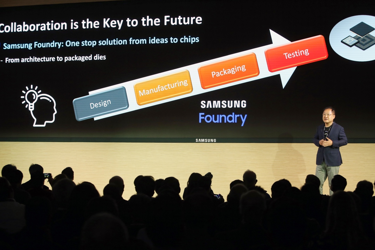
Samsung launches new foundry forum in Silicon Valley
By Song Su-hyunPublished : Oct. 18, 2019 - 15:21
Samsung Electronics said Friday it has launched a new forum in Silicon Valley as part of the efforts to enhance competitiveness of its foundry business.
Named as Samsung Advanced Foundry Ecosystem, or SAFE, the forum has been designed to provide an opportunity for Samsung’s partner companies to directly meet with customers and discuss comprehensive design technology infrastructure -- including electronic design automation, intellectual property, cloud, design service, and packaging -- which is critical to efficiently develop and manufacture semiconductor products.
Under the slogan “Partnering for a bold silicon future”, around 400 officials from the partner companies and customers gathered at the Samsung Device Solutions America office in San Jose on Thursday. The participants shared the latest chip design trends.
Samsung boasted its efficient and easy-to-use platform design infrastructure to the attendees.
As the latest system-on-chip products require more sophisticated features in a smaller surface size than before, the number of considerations in IC design optimization has increased exponentially, such as performance, power, security, design and density.
As a result, Samsung planned to host the new forum and announced it in March 2018.
In comparison with the existing Samsung Foundry Forum that has been held in different parts of the world every year, the SAFE Forum is aimed at allowing the partners to engage deeper and seek more efficient collaboration within Samsung’s foundry ecosystem by directly communicating with their customers, according to the company.
“The SAFE program has grown in quality over the past two years; it has expanded the number of competitive partnerships and support of flexible product design for customers as well as bolstered the relationship between our partners, customers, and Samsung foundry,” said Park Jae-hong, executive vice president of foundry design platform development at Samsung.
Samsung’s accelerating efforts to catch up with Taiwan’s TSMC, the world’s biggest foundry business, by aggressively expanding its capacity.
The Korean company is nearing completion of an extreme ultraviolet lithography line in Hwaseong, Gyeonggi Province, this year and will start operations next year.
While TSMC dominated the market with a 50.5 percent share as of the third quarter of 2019, Samsung accounted for 18.5 percent, according to data by market researcher TrendForce.
By Song Su-hyun (song@heraldcorp.com)
![[KH Explains] Hyundai's full hybrid edge to pay off amid slow transition to pure EVs](http://res.heraldm.com/phpwas/restmb_idxmake.php?idx=652&simg=/content/image/2024/04/18/20240418050645_0.jpg&u=20240419100350)
![[Today’s K-pop] Zico drops snippet of collaboration with Jennie](http://res.heraldm.com/phpwas/restmb_idxmake.php?idx=642&simg=/content/image/2024/04/18/20240418050702_0.jpg&u=)