
Most Popular
-
1
10-man S. Korea lose to Indonesia to miss out on Paris Olympic football qualification

-
2
Hybe-Ador feud should have limited effect on Hybe's overall performance: analysts

-
3
Second Gimpo civil servant found dead, after apologizing for not finishing work

-
4
DP leader says he will meet Yoon without conditions

-
5
First-ever meeting of president, opposition chief set to finally happen


-
6
NewJeans' singles, Japanese debut to proceed as planned, despite Hybe-Ador feud

-
7
Experts raise concerns about Japan putting pressure on Naver over Line

-
8
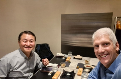
Samsung mobile chief, Google device head meet in Seoul
-
9
Blinken calls on China to press N. Korea to end its 'dangerous' behavior

-
10
Ship linked to NK arms shipments to Russia is moored in China: State Dept.


Samsung unveils next-generation memory solutions on Memory Tech Day
By Jie Ye-eunPublished : Oct. 21, 2023 - 03:02
Samsung Electronics unveiled its newest chip technologies and products at its annual global event in San Jose, California, Friday, eyeing a key role in providing hyperscale artificial intelligence models.
Under the theme of “Memory Reimagined,” about 600 people, including technicians, analysts and industry officials, attended this year’s Memory Tech Day to look into Samsung’s technologies in areas such as cloud, edge devices and automobiles.
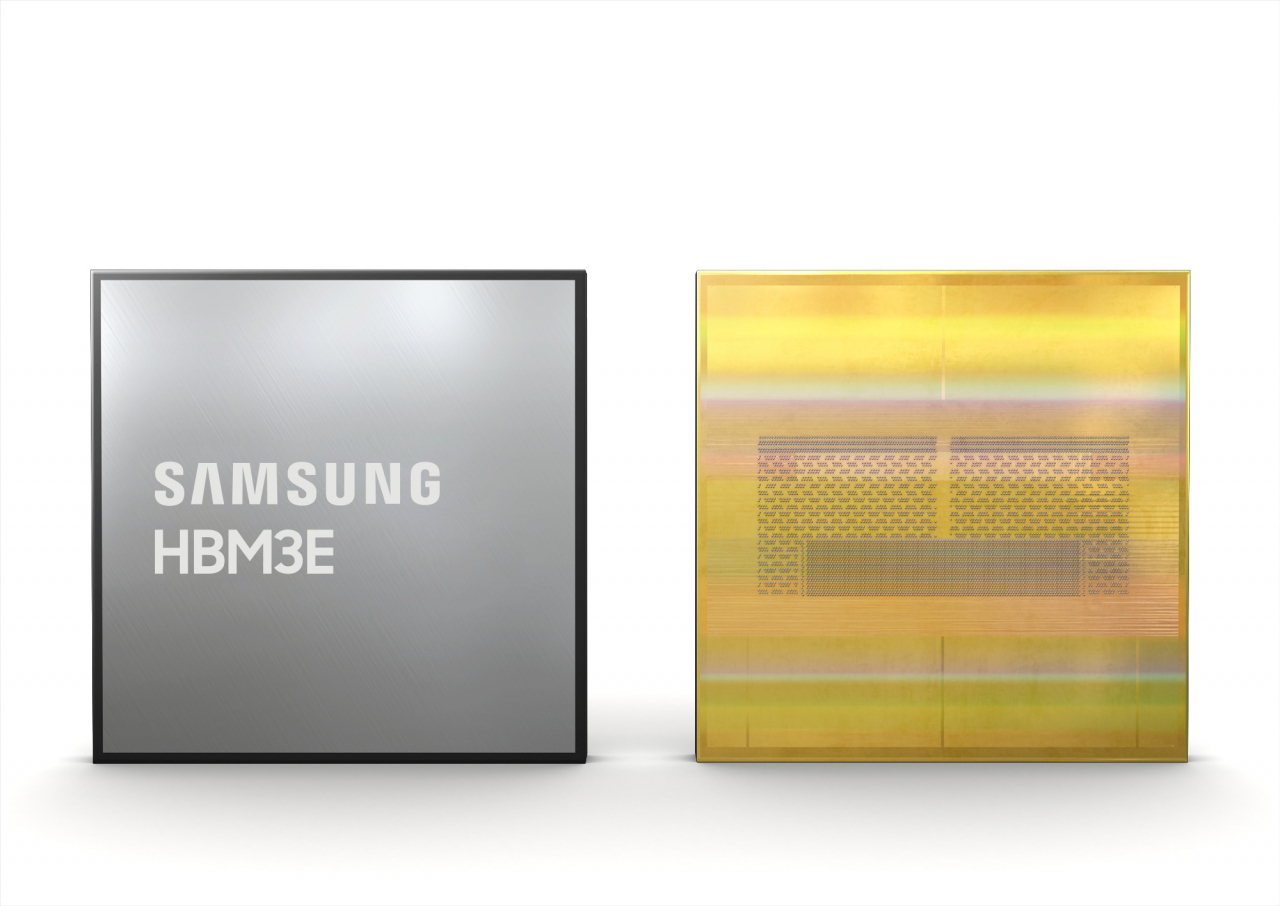
The tech giant unveiled its latest memory solutions, including the new fifth-generation HBM3e memory called Shinebolt; LPDDR package-based module LPDDR5X CAMM2 solutions and detachable AutoSSD that can be used through storage virtualization.
The Shinebolt provides high performance of up to 9.8 gigabits per second per data input and output pin, which can process over 1.2 terabytes per second. Samsung implemented high-level stacking by optimizing non-conductive film technology by filling gaps between chips.
Samsung’s industry-first 7.5Gbps LPDDR5X CAMM2 also captured attendees’ attention at Friday’s event. The chip threatens to be a game-changer in the next-generation PC and laptop DRAM market.
To achieve the No. 1 position in the memory market by 2025, it also introduced its Detachable AutoSSD, which supports continuous read speeds of up to 6,500 megabytes per second and provides 4TB of capacity.
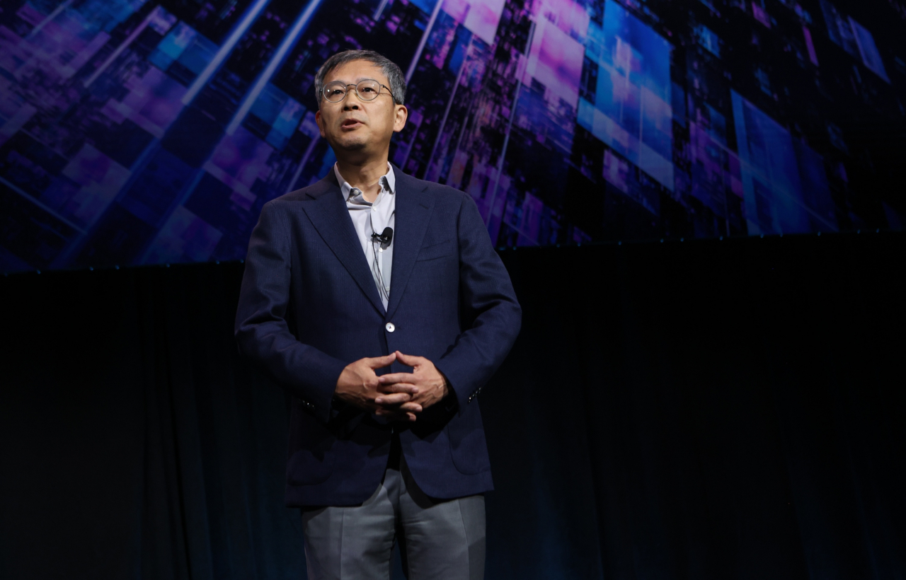
“The era of hyperscale AI models is a point where opportunities for technological innovation and growth meet together. It will be a time of challenge as well as greater leaps for the industry players,” Lee Jung-bae, executive vice president and head of US memory at Samsung Electronics said.
“We will continue to lead the memory market by providing expanded solutions that overcome limits through infinite imagination and bold challenges, alongside close cooperation with customers and partners,” he said, stressing the firm will introduce new structures and materials to overcome the challenges faced in the era of hyperscale AI models.
Samsung, which began mass production of 12-nano DRAM in May, announced that it was developing the next-generation 11-nano DRAM to achieve the industry's highest level of integration. The firm is also preparing to introduce a new 3D structure in DRAM of 10 nanometers or less and plans to expand the capacity to more than 100 gigabits on a single chip through this.
The tech giant also announced that has developed the highest number of layers that can be implemented with a double stack structure in the ninth-generation vertical NAND, or V-NAND. V-NAND is Samsung's name for 3D NAND.
It is working to reduce the planar area and height of cells to decrease volume and increase the number of layers through a key technology called channel hole etching, according to the company.
Samsung said its active participation in overcoming the global climate crisis through technology makes it sustainable through its cooperation with stakeholders, including customers and partners, within the entire semiconductor supply chain.